- 您现在的位置:买卖IC网 > Sheet目录364 > SST25VF010A-33-4I-QAE-T (Microchip Technology)IC FLASH SER 1MB 33MHZ SPI 8WSON
�� �
�
�1� Mbit� SPI� Serial� Flash�
�A� Microchip� Technology� Company�
�SST25VF010A�
�Data� Sheet�
�6.� Prior� to� any� Byte-Program,� AAI-Program,� Sector-Erase,� Block-Erase,� or� Chip-Erase� operation,� the� Write-Enable�
�(WREN)� instruction� must� be� executed.�
�7.� Block� addresses� for:� use� A� MS� -A� 15� ,� remaining� addresses� can� be� V� IL� or� V� IH�
�8.� To� continue� programming� to� the� next� sequential� address� location,� enter� the� 8-bit� command,� AFH,�
�followed� by� the� data� to� be� programmed.�
�9.� The� Read-Status-Register� is� continuous� with� ongoing� clock� cycles� until� terminated� by� a� low� to� high� transition� on� CE#.�
�10.� The� Enable-Write-Status-Register� (EWSR)� instruction� and� the� Write-Status-Register� (WRSR)� instruction� must� work� in�
�conjunction� of� each� other.� The� WRSR� instruction� must� be� executed� immediately� (very� next� bus� cycle)� after� the� EWSR�
�instruction� to� make� both� instructions� effective.�
�11.� Manufacturer’s� ID� is� read� with� A� 0� =0,� and� Device� ID� is� read� with� A� 0� =1.� All� other� address� bits� are� 00H.� The� Manufac-�
�turer’s� and� Device� ID� output� stream� is� continuous� until� terminated� by� a� low� to� high� transition� on� CE#�
�12.� Device� ID� =� 49H� for� SST25VF010A�
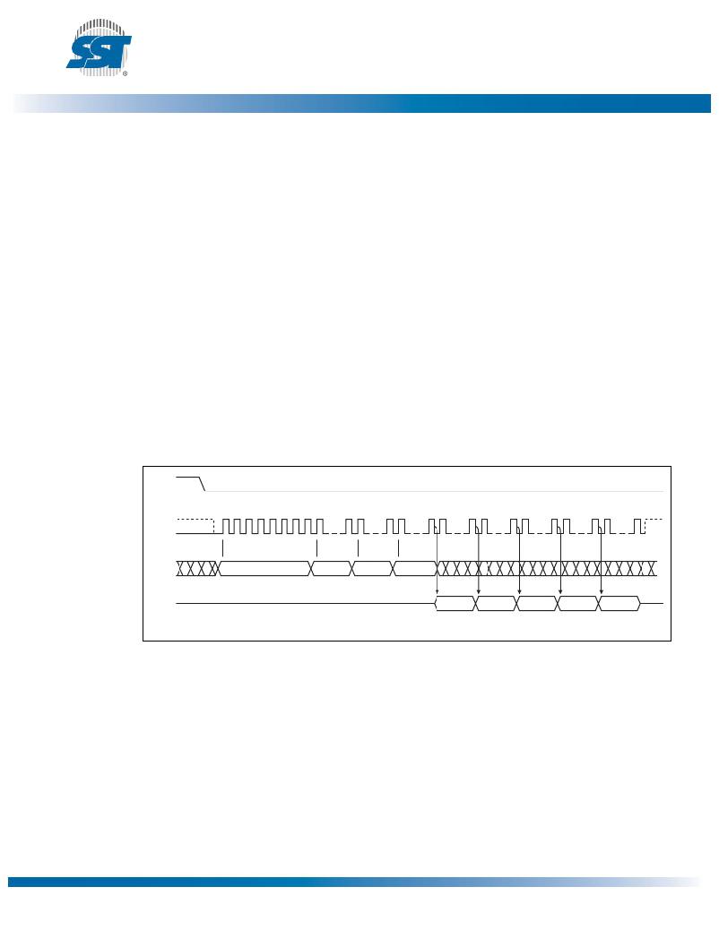
�Read� (20� MHz)�
�The� Read� instruction� outputs� the� data� starting� from� the� specified� address� location.� The� data� output�
�stream� is� continuous� through� all� addresses� until� terminated� by� a� low� to� high� transition� on� CE#.� The�
�internal� address� pointer� will� automatically� increment� until� the� highest� memory� address� is� reached.�
�Once� the� highest� memory� address� is� reached,� the� address� pointer� will� automatically� increment� to� the�
�beginning� (wrap-around)� of� the� address� space,� i.e.� for� 4� Mbit� density,� once� the� data� from� address� loca-�
�tion� 7FFFFH� had� been� read,� the� next� output� will� be� from� address� location� 00000H.�
�The� Read� instruction� is� initiated� by� executing� an� 8-bit� command,� 03H,� followed� by� address� bits� [A� 23� -�
�A� 0� ].� CE#� must� remain� active� low� for� the� duration� of� the� Read� cycle.� See� Figure� 4� for� the� Read�
�sequence.�
�CE#�
�MODE� 3�
�0� 1� 2� 3� 4� 5� 6� 7� 8�
�15� 16�
�23� 24�
�31� 32�
�39� 40�
�47�
�48�
�55� 56�
�63� 64�
�70�
�SCK�
�MODE� 0�
�SI�
�03�
�ADD.�
�ADD.�
�ADD.�
�SO�
�MSB�
�MSB�
�HIGH� IMPEDANCE�
�N�
�D� OUT�
�N+1�
�D� OUT�
�N+2�
�D� OUT�
�N+3�
�D� OUT�
�N+4�
�D� OUT�
�MSB�
�1265� F04.0�
�Figure� 4:� Read� Sequence�
�?2011� Silicon� Storage� Technology,� Inc.�
�10�
�S725081A�
�10/11�
�发布紧急采购,3分钟左右您将得到回复。
相关PDF资料
SST25VF016B-50-4C-S2AF-T
IC FLASH SER 16M 50MHZ SPI 8SOIC
SST25VF020-20-4C-QAE-T
IC FLASH SER 2MB 20MHZ SPI 8WSON
SST25VF020B-80-4C-QAE-T
IC FLASH SER 2MB 80MHZ SPI 8WSON
SST25VF032B-66-4I-S2AF
IC FLASH SER 32M 66MHZ SPI 8SOIC
SST25VF040B-50-4C-ZAE
IC FLASH SER 4MB 80MHZ SPI 8CSP
SST25VF040B-80-4I-QAE
IC FLASH SER 4MB 80MHZ SPI 8WSON
SST25VF064C-80-4I-Q2AE-T
IC FLASH SER 64M DUAL I/O 8WSON
SST25VF080B-80-4I-QAE-T
IC FLASH SER 8MB 50MHZ SPI 8WSON
相关代理商/技术参数
SST25VF010A-33-4I-SAE
功能描述:闪存 1M (128K x 8) 33MHz RoHS:否 制造商:ON Semiconductor 数据总线宽度:1 bit 存储类型:Flash 存储容量:2 MB 结构:256 K x 8 定时类型: 接口类型:SPI 访问时间: 电源电压-最大:3.6 V 电源电压-最小:2.3 V 最大工作电流:15 mA 工作温度:- 40 C to + 85 C 安装风格:SMD/SMT 封装 / 箱体: 封装:Reel
SST25VF010A-33-4I-SAE
制造商:Microchip Technology Inc 功能描述:MEMORY FLASH 1M SPI 8SOIC
SST25VF010A-33-4I-SAE_
制造商:Microchip Technology Inc 功能描述:
SST25VF010A-33-4I-SAE-T
功能描述:闪存 1M (128Kx8) 33MHz 2.7-3.6V Industrial RoHS:否 制造商:ON Semiconductor 数据总线宽度:1 bit 存储类型:Flash 存储容量:2 MB 结构:256 K x 8 定时类型: 接口类型:SPI 访问时间: 电源电压-最大:3.6 V 电源电压-最小:2.3 V 最大工作电流:15 mA 工作温度:- 40 C to + 85 C 安装风格:SMD/SMT 封装 / 箱体: 封装:Reel
SST25VF010A-33-4I-ZAE
功能描述:闪存 2.7V to 3.6V 1Mbit SPI Serial 闪存 RoHS:否 制造商:ON Semiconductor 数据总线宽度:1 bit 存储类型:Flash 存储容量:2 MB 结构:256 K x 8 定时类型: 接口类型:SPI 访问时间: 电源电压-最大:3.6 V 电源电压-最小:2.3 V 最大工作电流:15 mA 工作温度:- 40 C to + 85 C 安装风格:SMD/SMT 封装 / 箱体: 封装:Reel
SST25VF016B
制造商:SST 制造商全称:Silicon Storage Technology, Inc 功能描述:16 Mbit SPI Serial Flash
SST25VF016B_10
制造商:SST 制造商全称:Silicon Storage Technology, Inc 功能描述:16 Mbit SPI Serial Flash
SST25VF016B_11
制造商:SST 制造商全称:Silicon Storage Technology, Inc 功能描述:16 Mbit SPI Serial Flash